Table of Contents
| Table of Contents |
|---|
Child Pages
| Child pages (Children Display) |
|---|
Overview
Big ole network switch.
Current Status
Design Phase
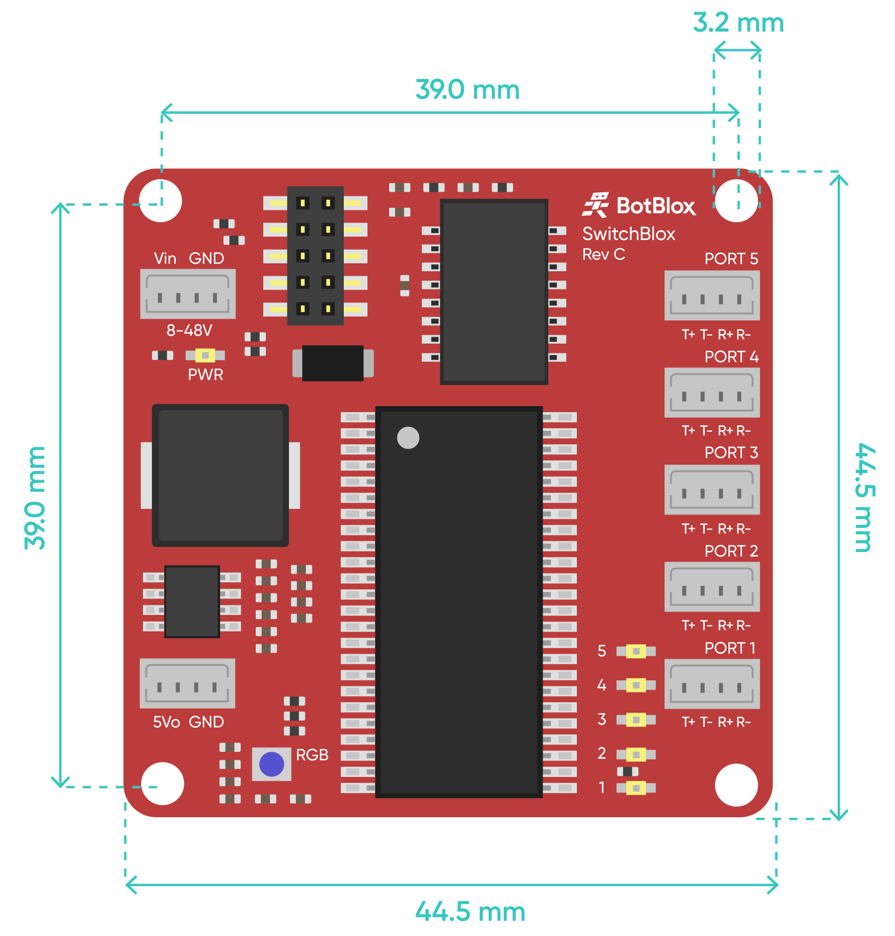
SwitchBlox 5-Port Ethernet Switch
Backplane Connector Pinout
Pinout
| Description | PIN | Description | |
|---|---|---|---|
| Battery Voltage | 1 | 2 | Battery Voltage |
| GND | 3 | 4 | GND |
| 5v | 5 | 6 | 5v |
| GND | 7 | 8 | GND |
| 3v3 | 9 | 10 | 3v3 |
| GND | 11 | 12 | GND |
| TX+ | 13 | 14 | RX+ |
| TX- | 15 | 16 | RX- |
| ADDR 0 (LSB) | 17 | 18 | ADDR 1 |
| ADDR 2 | 19 | 20 | ADDR 3 (MSB) |
| Power LED | 21 | 22 | Status LED |
| GPIO 0 | 23 | 24 | GPIO 1 |
| GPIO 2 | 25 | 26 | GPIO 3 |
| GPIO 4 | 27 | 28 | GPIO 5 |
| GPIO 6 | 29 | 30 | GPIO 7 |
Pin Description
Voltage Rails
Battery Voltage, 5V, and 3V3 rails are provided by the power module.
Ethernet
- RX/TX pairs are each tied to the output of the of the SwitchBlox Nano switch, so no crossover is necessary between RX and TX pins on the module.
LEDs
- Two LEDs are present on the Backplane for each module, allowing quick viewing of module status.
- The Power LED is a "loopback" LED indicating that a module is present. This pin should be shorted to the 3v3 voltage on each module. Alternatively, this LED pin can be pulled high by a microcontroller on the module upon receiving power.
- The Status LED is for any general indication of module status. This LED can be driven however the module owner sees fit.
- These LEDs will be disabled during flight via a jumper to save power.
Address pins
- Each module slot on the Backplane will have a unique address assigned to it. These pins will either be pulled to GND or 3v3 via 10k resistors to indicate to the module what the address is. (eg. all pins pulled to GND indicates module slot 0, ADDR0 at 3v3 indicates slot 1, etc.)
- These pins should be read by the module and used for purposes such as logging, verification of flight configuration, etc.
GPIO pins
- These pins are made available to each module such that there is little need for each module to have wires coming off in every which direction.
- The 8 GPIO pins and 1 GND pin will be broken out to a DE-9 connector on each end for each module. A pinout is shown below
| GPIO Pin | DE-9 Pin |
|---|---|
| GPIO 0 | 1 |
| GPIO 1 | 2 |
| GPIO 2 | 3 |
| GPIO 3 | 4 |
| GPIO 4 | 5 |
| GPIO 5 | 6 |
| GPIO 6 | 7 |
| GPIO 7 | 8 |
| GND | 9 |

(1)(1)(3).drawio.png?version=1&modificationDate=1677344841540&cacheVersion=1&api=v2&height=400)


