Why???
You might be wondering, "Hey Ben, why do we make our own parts from scratch if websites like UltraLibrarian and SnapEDA exist?" That is an excellent question! While it might seem much easier to just import a symbol + footprint from an external source like those, they usually do not conform to our standards. For example, most of the symbols you will find on there are ordered by pin layout, not by functionality which make for very ugly schematics. Additionally, we have all of our layers already set up in our footprint template (more on that later!), and the layers on downloaded footprints are usually all out of wack and require manual tuning which can be time consuming. In addition to our templates, Altium has tools that make symbol and footprint creation super easy, and conformant with IPC standards.
Symbol vs Footprint vs Component
With a software as complicated as Altium and the circuit design field in general, there is a lot of terminology that might be confusing to newcomers. Hopefully, this section will be able to clarify some of that.
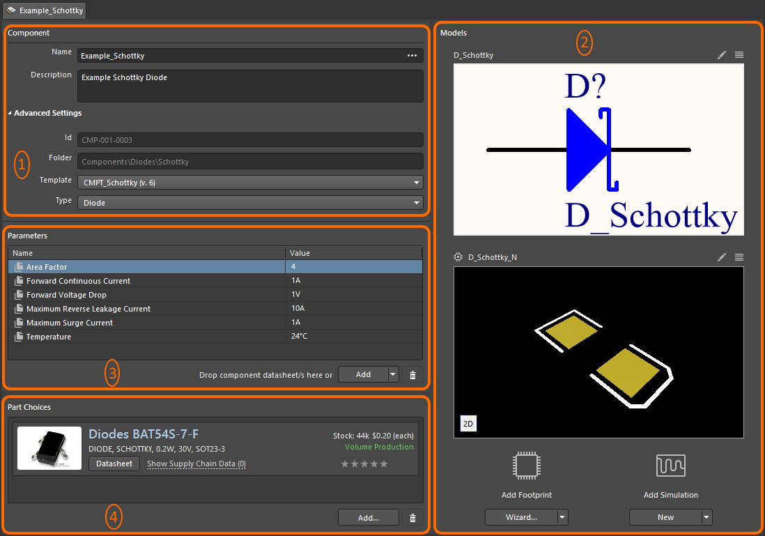
The three most important terms to know when creating a part in Altium are the symbol, footprint, and component. Each one of these plays an integral role in part creation, and you will need to become familiar with what each one means. In short, a symbol is the part that appears on your schematic, a footprint is the part that appears on your PCB layout (includes pads, markings, 3D body), and a component is what combines the symbol and footprint into a part for use and also includes other data like parameters, datasheets, and supplier information.
Most of the time with ICs a symbol will not map 1-to-1 with a footprint, so extra care needs to be taken that everything is mapped correctly according to the datasheet of the component you are trying to make. The below graphic visually shows the difference between a symbol and footprint.

Component Creation Screen:
File Structure
In Launch's Altium 365 workspace (Contact James May (RIT Student) for access if needed), all of our symbols, footprints, and components are located at a specific location. In order to access this location, you must use the Explorer panel in Altium. If it is not visible by default, click "Panels" in the bottom right and then check "Explorer" and drag it to the right to pin it. In the default library that Altium provides in the Explorer panel, our Launch specific library is located in Components > Models. Symbols are located in "Launch Symbols", footprints in "Launch Footprints", and components in "Launch Components". Files of the right type should be saved in the corresponding folder.
